|
United
Arab Emirates University
Faculty of Engineering
College Requirements Devision |
ENGINEERING
MATERIAL - (MECH 390)
NANO-STRUCTURED
MATERIAL
Section
No.
Prepared
By
Student
Name
ID
Student
Name
ID
Student
Name
ID
Supervising
Instructor: Dr. Raa Said
Dec.
20th, 2000
1.
Introduction
Nano-structured
materials have miniature crystal structure
that enables them to posses special properties.
Nano-structured materials are exceptionally
strong, hard, ductile at high temperatures,
wear-resistant, erosion-resistant, corrosion-resistant,
and chemically very active. This allows
the use of nanostructured materials in applications
that are of great importance to the advancement
of human life and technology. Although are
currently utilized in many application,
many aspects of nanostructured materials
are still under research and development
.
2.
What Are Nano-Structured Materials
Nano-structured
materials are those that have internal structural
elements (basic building blocks or crystals)
with a maximum dimension of few hundred
nano-meters. They are not different from
metals, ceramics, or polymers from classification
point of view, to the contrary, nano-structured
materials could be of any type but with
a crystal structure in the nano-meter range.
Since atoms average sizes are within few
Angstroms (1 Å = 10-10 m, a tenth
of a billion of a meter), one nano-meter
(1nm = 10-9 m) would be composed
of less that 10 atoms. Thus the grain size
of nanostructured materials are composed
of very few atom. This minute size of the
builiding block of nanostructured materials
provides them with many superior properties
when compared to conventional materials.
3.
Examples of Nano-structured Materials
Nanostructured
materials are encountered in many structures
and applications. For example paints, cosmetics,
powders, and pharmaceutical products are
all composed of nanostructured materials.
4.
Properties
The
properties of nanostructured materials are
dependent on several features, such as the
grain size and composition. Generally the
properties of the nanostructrued materials
show outstanding improvement or deviation
from the properties exhibited by the conventional
materials.
4.1
Mechanical properties:
Module
of elasticity:
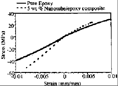
Figure
(1) shows a comparison between the stress-strain
behavior of pure epoxy and nanotube-epoxy
composite, it obvious that the module of
elasticity (E) for tension and compression
of the nanostructued material is higher.
Hardness:
Hardness
increases with the decreasing grain size,
for nanocrystalline pure metals (~ 10 nm
grain size) the hardness is 2 to 7 times
higher than those of larger grained (>1μ
m) metals.
Another
example is the nanophase copper and palladium
assembled from clusters with diameters in
the range 5-7 nm can have hardness and yield
strength values up to 500% greater than
in the conventionally produced metal.
 |
|
Fig.
1: The creep rate behavior for
1
|
Ductility:
Ductility
is strongly affected by the change in the
grain size. Ceramics which are usually
exhibit brittle behavior, are capable to
undergo appreciable plastic deformation
before fracture (ductility), in contrast
to the normal ceramics, which are normally
difficult to deform and hence very brittle
[3].
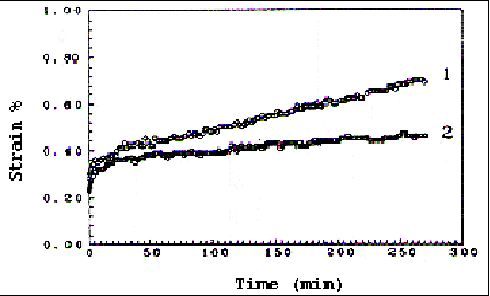
Creep:
Nanostructured
materials show different creep behaviors
than that of materials with those of conventional
grain size at different stress levels [2].
At high stresses nanostructured materials
creep rate is slower, but at lower stresses
and higher temperature, the creep behavior
is faster than the conventional material,
as shown in the figure (2) below.
|
|
|
Fig.
2: The Creep curves for Ni-20%P
alloy 1 is nanocrystalline, alloy
2 is conventional.
|
4.2
Electrical properties:
Nanostructured
materials have lower electrical resistance
than conventional material that have ordinary
grain size.
4.3
Magnetic properties:
Magnetic
nanoparticles show a variety of unusual
magnetic behaviors when compared to the
bulk materials.
Remanence:
Remanence
is magnitude of reflux density that remains
when a magnetic field is removed. Magnetic
nanoparticle shows a reduction in the remanence
behavior.
Coercivity:
It
is the applied magnetic field necessary
to reduce to zero the magnetic flux density
of magnetized material. Nanostructured
magnetic-materials posses coercivity 1-2
orders of magnitude higher than conventional
materials.
GMR
(Giant MagnitoResistance):
It
is a unique phenomena possessed by magnetic
nanostructured materials, which means reduction
of the electrical resistance of a material
when exposed to magnetic field, [4].
5.
Synthesis of Nano-structured Materials
There
are five widely known methods to produce
nanomaterials, and they are as follows:
-
Sol-gel synthesis,
-
Inert gas condensation,
-
Mechanical alloying or high-energy ball
milling,
-
Plasma synthesis, and
-
Electrodeposition.
All
these processes synthesize nanomaterials
to varying degrees of commercially viable
quantities. To date, of all the above process,
only sol-gel synthesis can produce materials
(both metals and ceramics) at ultra-low
temperature, large quantities relatively
cheaply, synthesize almost any material,
co-synthesize two or more materials simultaneously,
coat one or more materials onto other materials
(metal or ceramic particulates, and three-dimensional
objects), produce extremely homogeneous
alloys and composites, synthesize ultra-high
purity (99.9999%) materials, tailor the
composition very accurately even in the
early stages of the process, because the
synthesis is actually performed on an atomic
level, precisely control the microstructure
of the final products, and precisely control
the physical, mechanical, and chemical properties
of the final products.
6.
Typical applications
There
are typical different applications for the
nanostructure materials in different fields;
this is according to the enhancement it
does to certain properties as mentioned
above. Here is some of these applications:
6.1
Catalytic application:
Catalysts
are substances that increase the rate of
chemical reaction without being consumed
in the process. Catalysts are used in many
petroleum and petrochemical processes, chemical
separations, air separation applications,
and environmental clean up. In catalysis
the key goal is to promote reactions that
have high selectivity with high yield. It
is anticipated that this goal will be more
closely approached through tailoring a catalyst
particle via nanoparticle synthesis, that
it performs only specific chemical conversions,
performs these at high yield, and does so
with greater energy efficiency. In addition
to selectivity, the surface area is also
an important characteristic of catalyst,
high surface area can be attained by creating
materials where surface area is high compared
to the amount of the bulk support material.
Nanostructured
materials, such as zeolites, with their
potentially high surface areas compared
to conventional materials, make them suitable
for a variety of catalytic applications.
Beside that, the control of surface structure
at the nanostructure level makes it possible
to modify separation or catalytic process
selectivity by several orders of magnitude
[7].
6.2
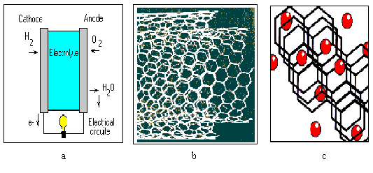
Fuel cell:
Fuel
cells are devices convert the chemical energy
directly to electrical energy. It operates
like battery, however it do not run down
or require recharging. Figure (3:A) below
shows one form of these cells in schematic
forms. A simple fuel cell consists of two
electrodes sandwiched around an electrolyte.
The anode receives the hydrogen steam and
the cathode receives the oxygen, generating
electricity, water and heat.
The
hydrogen atom splits into proton (which
passes through the electrolyte), and electrons
enters the electrical circuit.
One
obstruction in the usage of fuel cell, is
the storage of H2 , since it
require a large storage tank, nanoscale
materials or structure with exceedingly
high storage capacity per unit volume and
weight for gases such as H2 ,
is a solution for this problem. Carbon nanotube
which are cylindrical sheet of graphite
whose diameter is in nanoscale (2-20 nm),
is ideal storage media for hydrogen due
to their porous nature, and assumed capillary
forces which would serve to draw hydrogen
into the spaces between the carbon atoms
[7]. See Fig. 3b and 3c.
|
|
| Fig.
3: Illustration showing: (a) a fuel
cell schematic, (b) photomicrograph
of a carbon nanotube, and (c) Hydrogen
molecules stored in carbon nanotubes. |
7.
Advanced applications
7.1
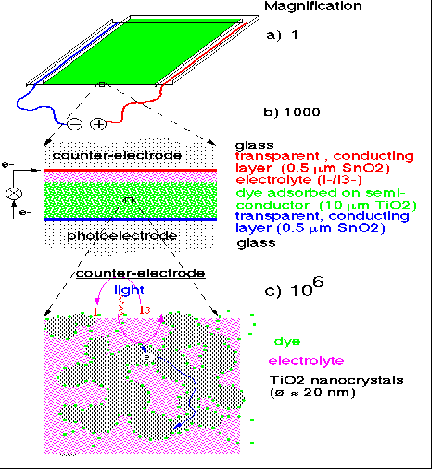
Nanostructured solar cell
Solar
cells are devices that convert the energy
of sunlight directly to electricity, they
made of semicanductors such as silicon.
A classic solar cell, see figure (4), consists
of two layers of semiconductor, one p-type
and the other n-type, sandwiched
together to form a pn junction.
The pn junction induces an electricity
field a cross the device. When particle
of light photons are absorbed by the semiconductor,
they transfer their energy to some of the
semiconductors electron , which are able
to move about through the material. For
each charged electron, a corresponding positive
charge is created known as a hole. The
movement of the electrons and holes across
the pn juncion induce a voltage across
the device. After a short time these electrons
and holes recombine [5].
In
nanostructured solar cell, a nanostructured
semiconductor with a high surface area is
used, rather than the flat semiconductor
in the classic solar cell, that result in
greater absorption of light and higher efficient
energy conversion. Furthermore, electron-hole
recombination in the semiconductor which
seriously affects the efficiency of classic
solar cell, dose not occur in this case
[6]. In figure (5), a schematic view of
the nanostuctured solar cell and its component.
7.2
Neural prostheses
Neural
prostheses is a surgical implants for patient
with neural damage (neuron is the brain
cell responsible for conducting the electrical
stimulus between cell). The damage of these
cells, result in inactivation of a portion
of the brain needed for normal daily activity.
Through this surgical implants the damaged
portion of the brain is electrically stimulate,
patient could then recover the lost function.
Compared
to conventional large grain-size materials,
nanophase materials exhibit improved current
capacitance, that is, the ability for a
material to conduct a current overtime.
Currently, the used materials have shorter
lifetime, and thus they require a frequent
replacement. Neural prostheses composed
of nanostructured materials, which has the
ability to electrically stimulate other
neurons longer, and that eliminates the
repeated need for surgical replacement.
|
|
|
Fig.
4: Typical solar cell layer structure.
|
|
|
|
Fig.
5:Illustration of the Nanostructured
solar cell.
|
8.
Current Status
Currently
nanostructured materials are under extensive
development and investigation. Due to their
processing and remarkable range of application,
there is a wide range of disciplines contributing
to the developments in nanostructure science
and technology worldwide. Each year sees
an ever-increasing number of researchers
from diverse disciplines enter the field
and an increasing breadth of novel ideas
and exciting new opportunities explode on
the international nanostructure scene.
The
rapidly mounting level of interdisciplinary
activity in nanostructuring is truly exciting.
The intersections between the various disciplines
are where much of the novel activity resides,
and this activity is growing in importance.
Current reserches are focused on developing
new synthesis routes of nanostructured metals,
nanostructured ceramic, nanostructured polymers
and their composite.
The
properties of this materials (i.e. electrical,
magnetic, mechanical, optical
.. etc) are
comprehensively under study. New applications
for this material is also under progress,
example are nanoparticle fillers in metal,ceramic,
or polymer matrices, which can yield a very
wide range of nanocomposites with unique
properties.
Nanoscale
devices are also under development. One
of the major researches and development
effort worldwide in nanoscale devices is
focused on the magnetic devices using Giant
MagnetoResistance (GRM), which is the decrease
of electrical resistance of materials when
exposed to a magnetic field.
9.
Future Issues
Nanotechnolgy
is the creation and utilization of material,
devices, and systems through the control
of matter on the nanometer length scale,
that is, at the level of atoms and molecule.
This new founded field is a natural result
of the nanostructured materials and there
use in different applications. All natural
materials and systems establish their foundation
at the nano-scale. The control of matter
at molecular levels means tailoring and
manipulating the fundamental properties,
and processes exactly at the nano-scale,
where the basic properties are determined.
Nanotechnology
will be a strategic branch of science and
engineering for the current century, thus
there would be unbounding restructure for
the technologies currently used for manufacturing,
medicine, defense, energy production, environmental
management, transportation, communication,
computation and education, thus the nano-science
and engineering will most likely produce
the breakthrough of tomorrow.
One
of the outstanding application of nanotechnology
(molecular manufacturing), is the building
of central processing unit (CPU) for a computer
that occupies a volume less than 1 cubic
micrometer, consumes roughly 100 nanowatts
of power, and executes about 1 billion instructions
per second (1 GHz).
In
the medical field, the application of molecular
manufacturing will lead to development of
nanoscale medical devices of greater complexity
and capability than modern drug molecules,
and of far greater precision than modern
surgical instruments. More information
about this topic, is available in references
[9] and [10].
References
[1] http://www.rci.rutgers.edu/~majohnm/nanomat.html.
[2] http://www.rpi.edu/~crawfp/nano/.
[3] http://www.itri.loyola.edu/nano/06-01.htm.
[4] http://www.itri.loyola.edu/nano/06-03.htm.
[5] http://www.pv.unsw.deu.au/info/solarcel.html.
[6] http://www.epfl.ch/icp/ICP-2/solarcell-E.html.
[7] H. Gleiter, Nanostructured materials:
Basic Concepts and Microstructure, Acta
Materialia 48, pages 1-29, 2000.
[8] Mc GRAW-HILL, Encyclopedia of Science
and Technology. 8th edition,
pages 624- 627.
[9] K.Eric and Chris, Unbounding the
Future: The Nanotechnology Revelution.
William Morrow and Company Inc., New York,
1991.
[10]
B.C. Crandall, Nanotechnology. Massachusetts
Institute of Technology, London, 1996.
|